Multi-Layer PCB Circuit Board Multi-Layer Printing PCB Board
Product Description
| Materials | FR-4/HTG150-180 FR-4/CEM-1/CEM-3/Aluminum |
Number of Layer | 1-32 layers (include Rigid-Flex PCB) |
| Board Thickness | Rigid 0.2-4.0mm, Flex 0.01-0.25mm |
| Board Thickness Tolerance | 5-10% |
| Board Cutting | V-cut,Routing |
| Copper Weight | 0.2oz-10oz |
| Copper Weight Tolerance | ±0.15 oz |
| Copper Thickness | 0.5oz-5oz |
Min Trace Width | 0.15mm |
Min Space Width | 0.15mm |
Min Drill Hole Diameter | 0.1mm |
Silk Screen Min Line Width | 0.15mm |
Soldermask | green,red,blue,white,black,yellow,etc. |
| Flame resistance | 94v0 |
| Certification | ISO 9001:2000,ISO 14001,ISO/TS16949:2002,UL E203640 |
| Suface Finish | HASL/Nickle/Lead Free HASL/OSP/Gold Plating/Immersion Gold/ENIG/Rosin etc |
Detailed Terms for Pcb Assembly
Quantity | Prototype&sample PCB Assembly, Small and middle mass prodution is our specialty and we also can handle the orders up to 2000. |
Type of Assembly | THD (Thru-Hole Device), SMT (Surface-Mount Technology), Double-sided SMT & THD mixed |
Solder Type | Water Soluble Solder Paste,Leaded and Lead-Free. |
Components | Passives parts, smallest size 0201; |
Bare Board Size | Smallest: 0.25x0.25 Inches; Largest: 20x20 Inches. |
File Formats | Bill of Materials Gerber Files Pick-N-Place File(XYRS). |
Type of Service | Turn-Key, Partial Turn-Key or Consignment. |
Component Packaging | Reels,cut tape,Tube and tray,Loose parts and bulk. |
Turn Time | 3 - 10 days |
Testing | X-ray Inspection |
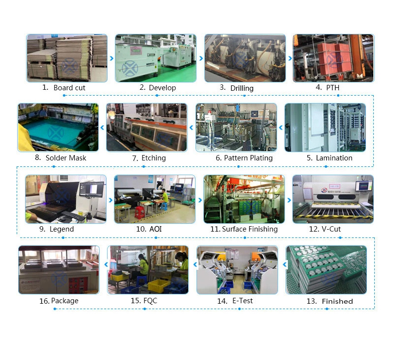
PCB Production Process:
Our advantages

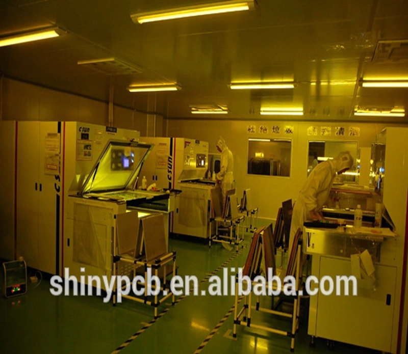
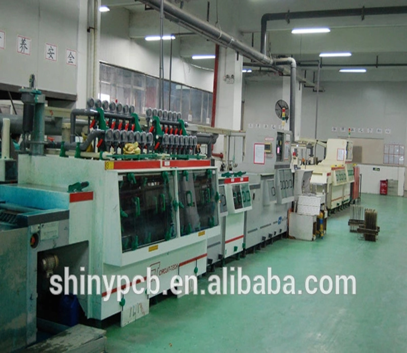
Workshop equipment


FAQ
Q1:What service do you have?
A1: One-stop service including PCB production + Component sourcing + Assembly
Brand of material
Q2: What material brand you use for your PCB?
A2: KB, SL, NANYA, TACONIC, ROGERS and so on.
MOQ
Q3: What is your minimum order quantity?
A3: We have no limitation on MOQ, prototype, medium volume and large volume are all acceptable.
Q4:What files required to get quotation from you?
A4: For PCB quotation, please provide the Gerber data/files and indication of related technical requirements as well as any special requirement if you have.
For PCBA quotation, please provide Gerber data/ files and also BOM (bill of materials), and if you need us to do function test, please also provide the test instruction/procedure.