Shenzhen LvMeiJinYu Electronic Co.,Ltd


1. Process capacity
2. Lead Time

3. Major Equipment

3. Main Customers

Any question, Pls contact us,Thank you!
Founded in 2005 and headquartered in Shenzhen, LM devotes to technology innovation and covers industries of telecommunication,power, security, Optronics, industrial control, medical, Auto product, comsumer electronics, etc., 40% product for oversea market of South America, Europe, Japan, India, Middle East, etc..
Each year, we complete thousands of successful assignments, this volume creates market knowledge that allows us to seize opportunities, speed the business process and create the most thorough, precisely accurate picture of PCB & related industries conditions and trends.
Every day, in markets around the globe, we apply our insight, experience, intelligence and resources to help customers make informed PCB & related services/products decisions.


1. Process capacity
| NO | Item | Capabilities |
| 1 | Number of Layers | 2-20 layers |
| 2 | Finished Board Size(Max) | 21.5″×24.5″(546mm×622mm) |
| 3 | Finished Board Thicknes | 0.126″- 0.016″ (0.3mm-3.2mm) |
| 4 | Finished Board Thickness Tolerance | ±10% ±3mil (board thickness≤ 0.8mm) Board Thickness ≤ 0.8mm |
| 5 | Warp age(Min) | ≤0.7% |
| 6 | Drill Hole Diameter | 0.005"-0.255" (0.15mm~6.5mm) |
| 7 | Base Copper Thickness of Outer Layer | 1/3 OZ-3OZ (0.012mm -0.102mm) |
| 8 | Base Copper Thickness of Inner Layer | 1/2 OZ-3 OZ (0.017mm -0.105mm) |
| 9 | Type of Base Material | FR-4 (130ºCTg-180ºCTg),CEM3,etc |
| 10 | Aspect Ratio of Plated Hole(Max) | 10:01:00 |
| 11 | Hole Diameter Tolerance(PTH) | ±3mil ( ±0.075mm) |
| 12 | Hole Diameter Tolerance(NPTH) | ±1mil ( ±0.025mm) |
| 13 | Copper Thickness of PTH Wall | ≥0.8mil (≥0.020mm) |
| 14 | Design Line Width/Space of Inner Layer(Min) | H/HOZ 3.0mil/3.0mil(0.075mm /0.075mm) 1/1OZ 4mil/4mil(0.1016mm/ 0.1016mm) 2/2OZ 5mil/5mil(0.127mm/0.127mm) |
| 15 | Design Line Width/Space of Outer Layer(Min | T/TOZ 3.0mil/3.0mil (0.075mm/ 0.075mm) H/HOZ 3.5mil/3.5mil(0.089mm/0.089mm) 1/1OZ 4.5mil/4.5mil (0.114mm/0.114mm ) 2/2OZ 6mil/6mil (0.152mm/0.152mm ) 3/3OZ 7mil/7mil (0.152mm/0.152mm) |
| 16 | Solder Mask Bridge(Min) | 2. 5mil (0.064mm) |
| 17 | Dimension Tolerance (Hole to Edge)(Min) | ±4mil ( ±0.101mm) |
| 18 | Thermal Shock | 288 ºC 10secs(3times) |
| 19 | Ionic Contamination | <1.56ug/cm2(NaCl) |
| 20 | Peel Strength | ≥1.4N/mm |
| 21 | Natural Impedance Control | ±10% |
| 22 | Solder Mask Strength | >6H |
| 23 | Surface Treatmet | Nickel /Gold Plating, HASL(Lead-free), OSP, ENIG, Immersion Silver, Carbon Oil, Peelable Mask, etc. |
2. Lead Time

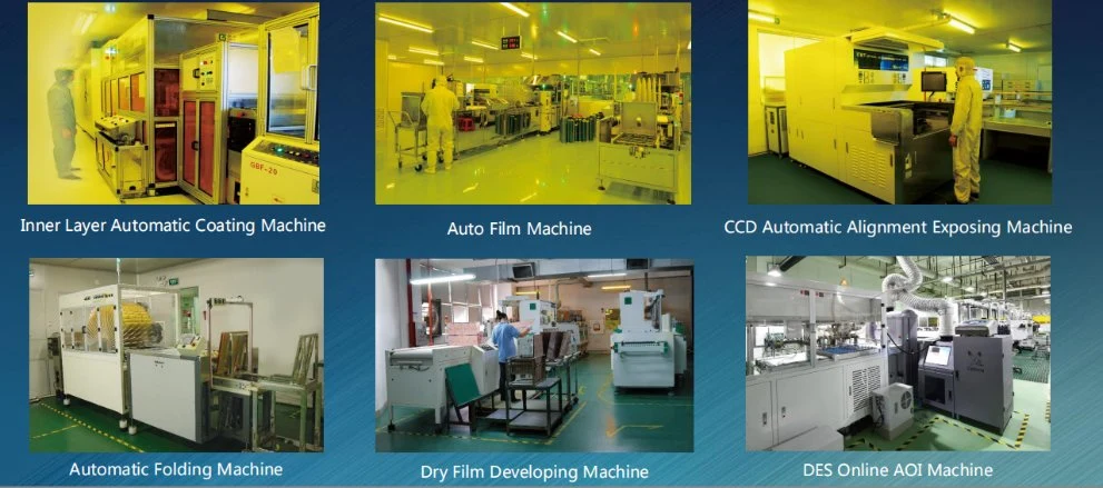
3. Major Equipment

3. Main Customers

Any question, Pls contact us,Thank you!